Skip to content
No results
  • About Us
  • PCB Segment
    • Introduction PCB Segment
    • Environmental Protection
    • Policy – Labor, Environment, Health& Safety and Ethics
    • Job Opportunities
  • PCB Solutions
    • Introduction PCB Solutions
    • Reliability
    • Product & Processes
  • Product
  • Our Client
  • Contact
    • Global Support
    • Contact Us
  • CN
Top Search

VOP/VIP

Capability of VOP plugging

Max Via hole
0.6 mm
Max panel thickness
5 mm
Aspect Ratio
<= 8:1


Via-on-pad product cross-section
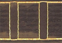
VOP plugging result

相关产品

  • Heavy Copper

    Read more
  • Hybrid Construction

    Read more
  • HDI Technology

    Read more

About Us

Founded in 1985, Topsearch has established itself as a pioneer in PCB manufacturing. In 1987, we set up state-of-the-art PCB manufacturing facilities in China. Our production facilities were strategically established in Shekou, Shenzhen, and commenced operations in 1988.

About Us

Founded in 1985, Topsearch has established itself as a pioneer in PCB manufacturing. In 1987, we set up state-of-the-art PCB manufacturing facilities in China. Our production facilities were strategically established in Shekou, Shenzhen, and commenced operations in 1988.

©Copyright 2025 by Topsearch, All rights reserved.

Legal Information